The U.S. Army Communications-Electronics Command’s Tobyhanna Army Depot opened a new microelectronics manufacturing facility in June 2025 to develop repair, manufacturing, and testing capabilities for circuit card requirements by complex military systems. Few know that the very foundation of printed circuit boards traces its history to one of CECOM’s predecessor organizations, the Signal Corps Engineering Laboratories, and the pioneering and innovative work conducted there after World War II.
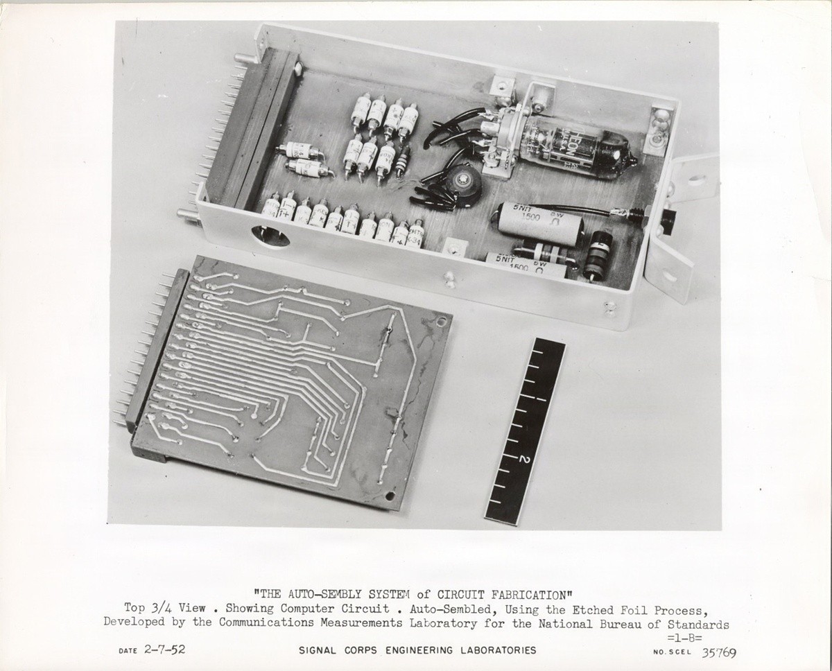
First developed in 1949 by two Signal Corps scientists, Moe Abramson and Stanislaus F. Danko, the “Auto-sembly” process punched holes in regular printed or etched electronic circuits, then dropped the component leads through the holes and dipped in a solder bath, soldering all connections in a single operation. With the development of board lamination and etching techniques, the concept evolved into the standard process for printed circuit board fabrication. The Army received the patent for this innovation in 1956.
Printed circuit techniques were promoted in 1947 in the National Bureau of Standards Circular 468. That publication stated, “Printed electronic circuits are no longer in the experimental stage. Introduced into mass production early in 1945 in the tiny radio proximity fuze for mortar shells developed by the National Bureau of Standards, printed circuits are now the subject of intense interest of manufacturers and research laboratories in this country and abroad.” Printed circuits were produced on an insulated surface by one of six techniques: painting, spraying, chemical deposition, vacuum processes, die-stamping, or dusting.
In an article titled “Auto-sembly of Miniature Military Equipment,” printed in the July 1951 edition of Electronics Magazine, the authors Danko and S.J. Lanzalotti explain the evolution of the technique, first experimenting with chemically etched printed circuit boards in 1949, which arose from the process used by nameplate manufacturers to create signs. “The system designated as Auto-sembly borrows the very convenient prefabricated conductor pattern of printed circuits and permits rapid and effective electrical combination of this pattern with conventional quality components by a one-shot solder dip process. The elements of Auto-Sembly are: (1) Formation of the conductor pattern; (2) selection of components; (3) rapid assembly; (4) packaging.”
The benefits of the system were clearly laid out. The mobilization advantages included:
- Saving Labor by eliminating manual wiring,
- Minimizing rejects due to the increased uniformity of etched wiring,
- Eliminates unsoldered joints because all joints are made simultaneously in one solder-dip operation,
- Reduces inspection time because mechanization reduces errors,
- Speeds assembly time with no hook or wrap-around joints,
- Permits greater miniaturization due to compact etched wiring, which lends itself to the stacking of chassis layers,
- Improves reliability by eliminating short-circuits between connections and lead.
The process remains relevant today, and the innovations of the “auto-sembly” process were transformative for both the military and commercial enterprises.
Social Sharing